news

IBM Debuts World's First Sub-1 Nanometer Chip Technology

Jun 25, 2026 · Source: cision
IBM Debuts World's First Sub-1 Nanometer Chip Technology

Built with revolutionary "nanostack" 3D chip architecture, IBM's sub-1 nm chip to propel semiconductor industry forward for the next decade

YORKTOWN HEIGHTS, N.Y., June 25, 2026 -- IBM (NYSE: IBM) today unveiled a major semiconductor breakthrough with the introduction of the world's first sub-1 nanometer (nm) chip technology, featuring a revolutionary transistor architecture at the 0.7 nm, or 7 angstrom node. The achievement marks a landmark moment for an industry facing the physical limits of traditional chip scaling. Semiconductors play critical roles in everything from computing, to appliances, to communication devices, transportation systems, and critical infrastructure.
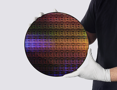
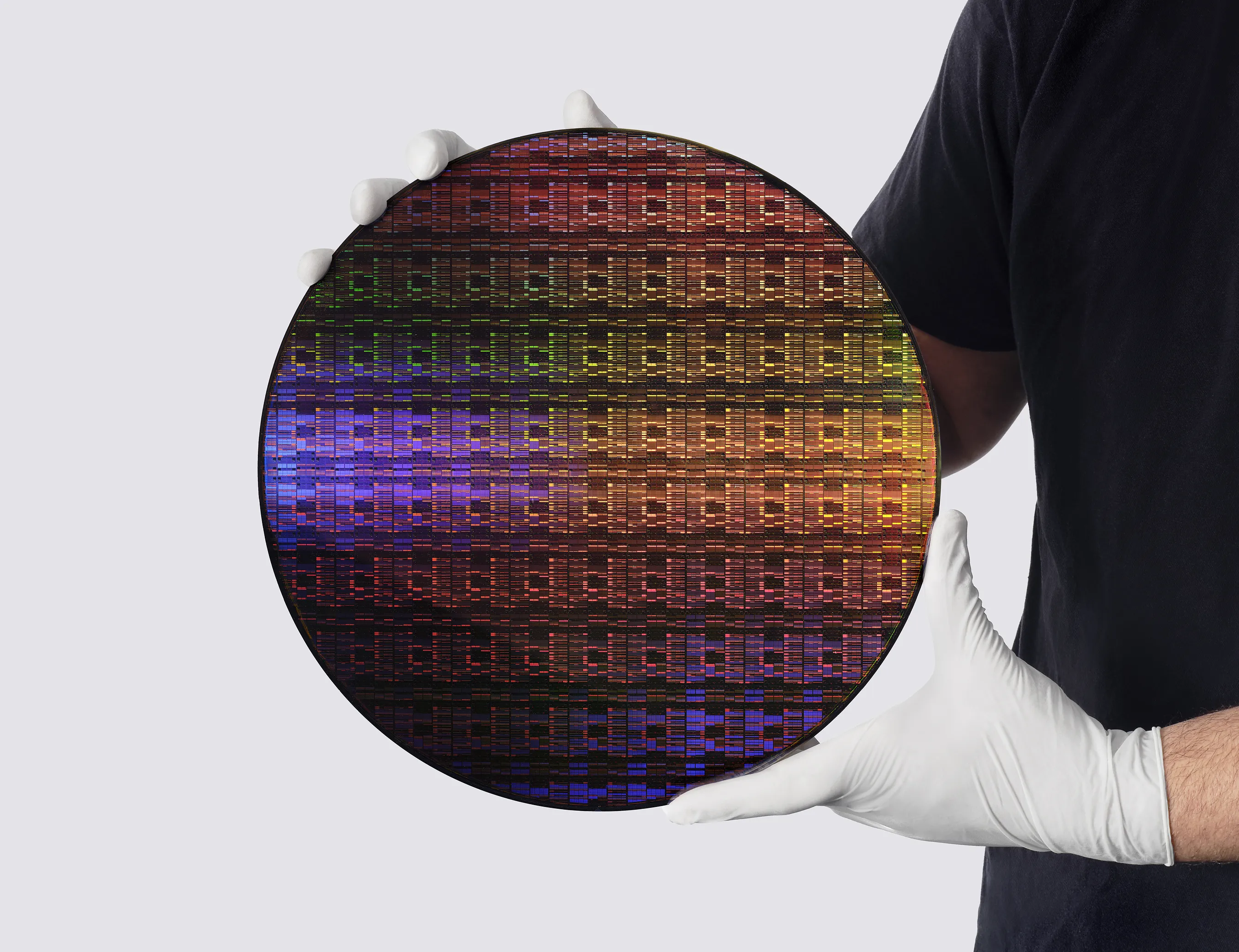
IBM's sub-1 nanometer node wafer. (Credit: IBM)

IBM's new sub-1 nm chip packs nearly 100 billion transistors onto a chip the size of a fingernail, nearly twice the density of IBM's 2 nm chip, unveiled in 2021. Enabled by a series of structural and material innovations, including IBM's groundbreaking three-dimensional nanostack architecture, the technology demonstrates how continued gains in performance and efficiency remain possible even as chip features approach atomic dimensions. 

Published technical results report the new chip is projected to offer a substantial leap in capability—up to 50 percent more performance, or 70 percent greater energy efficiency than IBM's 2 nm node chips1—supercharging compute for applications ranging from generative AI and cloud infrastructure to next-generation electronic devices.

"IBM's latest chip breakthrough marks a landmark moment in computing, pushing technology beyond the nanometer era to the scale of atoms. With our new nanostack architecture, we're not just making smaller transistors, we're reinventing how chips are built to deliver dramatically more power and energy efficiency," said Jay Gambetta, Director of IBM Research and IBM Fellow. "This industry-first innovation continues IBM's legacy of leading in next-generation technologies and sets the foundation for the next era of computing."

Nanostack, an Industry Breakthrough in Chip Design

To produce this chip, IBM researchers developed an entirely new transistor architecture, called "nanostack," the industry's first known three-dimensional, nanosheet-based design. Nanostack represents a major advance beyond nanosheet technology, the industry's current leading-edge architecture, invented by IBM. The nanostack design vertically stacks and staggers transistors, taking advantage of 3D sequential integration to pack more transistors onto a chip. The design also unlocks the use of different material combinations within each stacked layer, optimizing performance and power efficiency of each transistor independent of the other.

IBM's nanostack architecture was experimentally validated through ultra-thin dielectric bonding in CMOS integration, demonstration of dual-channel engineering capability, and functional CMOS inverter operation with expected switching performance. Together, these results confirm the nanostack technology can be physically built and supports real computation.

Additionally, in new research presented at VLSI 2026, IBM researchers demonstrated that the nanostack architecture provides 40 percent scaling in SRAM,2 unlocking the ability of chip designers to create much more efficient chips while also supporting the high-bandwidth data demands of advanced AI workloads.

With this groundbreaking structure, logic technology can extend for the first time below the 1 nm node, advancing the era of angstrom-level scaling, where dimensions approach the size of individual atoms. While transistor nodes now refer to a generation of manufacturing technology versus an exact physical dimension, IBM's 0.7 nm technology—also referred to as 7 angstroms—demonstrates how continued scaling remains possible. With the new nanostack architecture, IBM's semiconductor roadmap projects at least a decade of future scaling.

Building on Decades of Leadership in Semiconductor Innovation

This breakthrough is the latest testament to IBM as a leader in semiconductor R&D. IBM has led the world in developing the chips that power computing systems for decades, from early semiconductors in the 1960s to the world's first 2 nm node chip. IBM continues to innovate at the cutting edge of silicon, AI hardware, logic, and quantum processors developed to power the future of computing.

IBM and its partners conduct this work at a leading semiconductor research facility in Albany, New York, which will soon be home to a High Numerical Aperture Extreme Ultraviolet (High NA EUV) lithography tool, essential for the future of logic scaling. Developed by ASML, this technology enables ultra‑precise circuit printing, supporting the creation of smaller, more powerful chips. IBM and partners including Lam Research Corp., Tokyo Electron (TEL), and SCREEN Semiconductor Solutions, Ltd. have been working together to develop new High NA EUV processes and tools that have already yielded working devices.

IBM also recently announced a plan to form Anderon, the world's first pure-play quantum foundry. Anderon, a standalone IBM company, will draw on IBM's industry-leading quantum computing and semiconductor expertise to help position the United States to manufacture most of the world's quantum wafers.

With the expectation of the earliest adoption of nanostack technology at the sub-1 nm node, IBM sees a path to production in as early as the next 5 years.

About IBM

IBM is a leading provider of global hybrid cloud and AI, and consulting expertise. We help clients in more than 175 countries capitalize on insights from their data, streamline business processes, reduce costs and gain the competitive edge in their industries. More than 4,000 government and corporate entities in critical infrastructure areas such as financial services, telecommunications and healthcare rely on IBM's hybrid cloud platform and Red Hat OpenShift to affect their digital transformations quickly, efficiently and securely. IBM's breakthrough innovations in AI, quantum computing, industry-specific cloud solutions and consulting deliver open and flexible options to our clients. All of this is backed by IBM's long-standing commitment to trust, transparency, responsibility, inclusivity and service. Visit www.ibm.com for more information.

Media Contacts

Willa Hahn

IBM Communications

willa.hahn@ibm.com

Brittany Forgione

IBM Communications

brittany.forgione@ibm.com

1 S. Reboh et al "NanoStack Transistor Architecture for CMOS 7A Node and Beyond" VLSI 2025

2 Chen Zhang et al "Area and Performance of Staggered-Channel Nanostack SRAM Bitcells" VLSI 2026
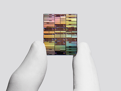
IBM's sub-1 nanometer node chip. (Credit: IBM)

IBM Corporation logo.

Cision View original content to download multimedia:https://www.prnewswire.co.uk/news-releases/ibm-debuts-worlds-first-sub-1-nanometer-chip-technology-302809990.html


Comments (0)

Login to join the conversation

Login / Register

No comments yet. Be the first to comment!

More to Read

Tredence Launches Domain Native Forward Deployed Engineering to Close the Last Mile of Enterprise AI
news
Jul 27, 2026 1 min

Tredence Launches Domain Native Forward Deployed Engineering to Close the Last Mile of Enterprise AI

The FDE practice builds an elite class of engineers at the intersection of domain expertise and data & AI, solving enterprises hardest business problems. BENGALURU, India and SAN JOSE, Calif. , July 27, 2026 -- Tredence, the world s leading data & AI services company, today announced the launch of its Forward Deployed Engineering (FDE) practice, committing to build a dedicated pool of 200 FDEs over the next 12-18 months. Through this practice, the company intends to build the most domain-native engineering capability in the market, helping clients move faster from problem to impact.

Mapex AI Accelerates Global Growth in Geospatial Intelligence through Strategic Government Projects and International Partnerships
news
Jul 27, 2026 1 min

Mapex AI Accelerates Global Growth in Geospatial Intelligence through Strategic Government Projects and International Partnerships

NOIDA, India , July 27, 2026 -- Mapex AI Private Limited, a leading geospatial technology company, continues to strengthen its global presence by delivering innovative, enterprise-grade geospatial solutions that transform complex spatial data into actionable intelligence. The Company has developed deep expertise in delivering GIS-based Master Planning, Land Information Systems, Property Tax Solutions, Utility Mapping, Digital Twins, Navigation, High-Precision Surveys, Enterprise GIS, and Geospatial Data Infrastructure to support India s flagship digital governance and infrastructure programmes.

Highstar Launches Full-Chain Battery Cell Portfolio for AI Data Centers
news
Jul 27, 2026 1 min

Highstar Launches Full-Chain Battery Cell Portfolio for AI Data Centers

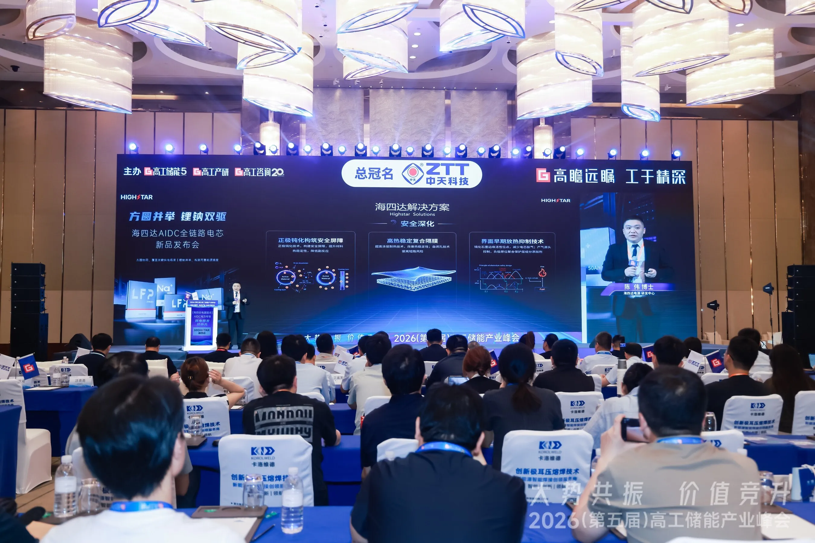
NANTONG, China , July 27, 2026 -- Highstar unveiled its full-chain battery cell solution for artificial intelligence data centers (AIDCs) at the 2026 GGII Energy Storage Industry Summit. The portfolio spans three critical power layers: grey-space UPS and high-voltage direct current (HVDC) systems, white-space battery backup units (BBUs), and grid-side energy storage. Targeted cells for grey-space and white-space challenges As AI workloads increase rack density and load volatility, data centers require faster response, dependable backup, controlled temperature rise and stronger lifecycle performance. Highstar s solution centers on two products for the layers closest to computing loads.

Ookla Study in Manila: Carrier VoLTE Networks Prove to Outperform OTT Apps in Voice Quality and Reliability
news
Jul 27, 2026 1 min

Ookla Study in Manila: Carrier VoLTE Networks Prove to Outperform OTT Apps in Voice Quality and Reliability

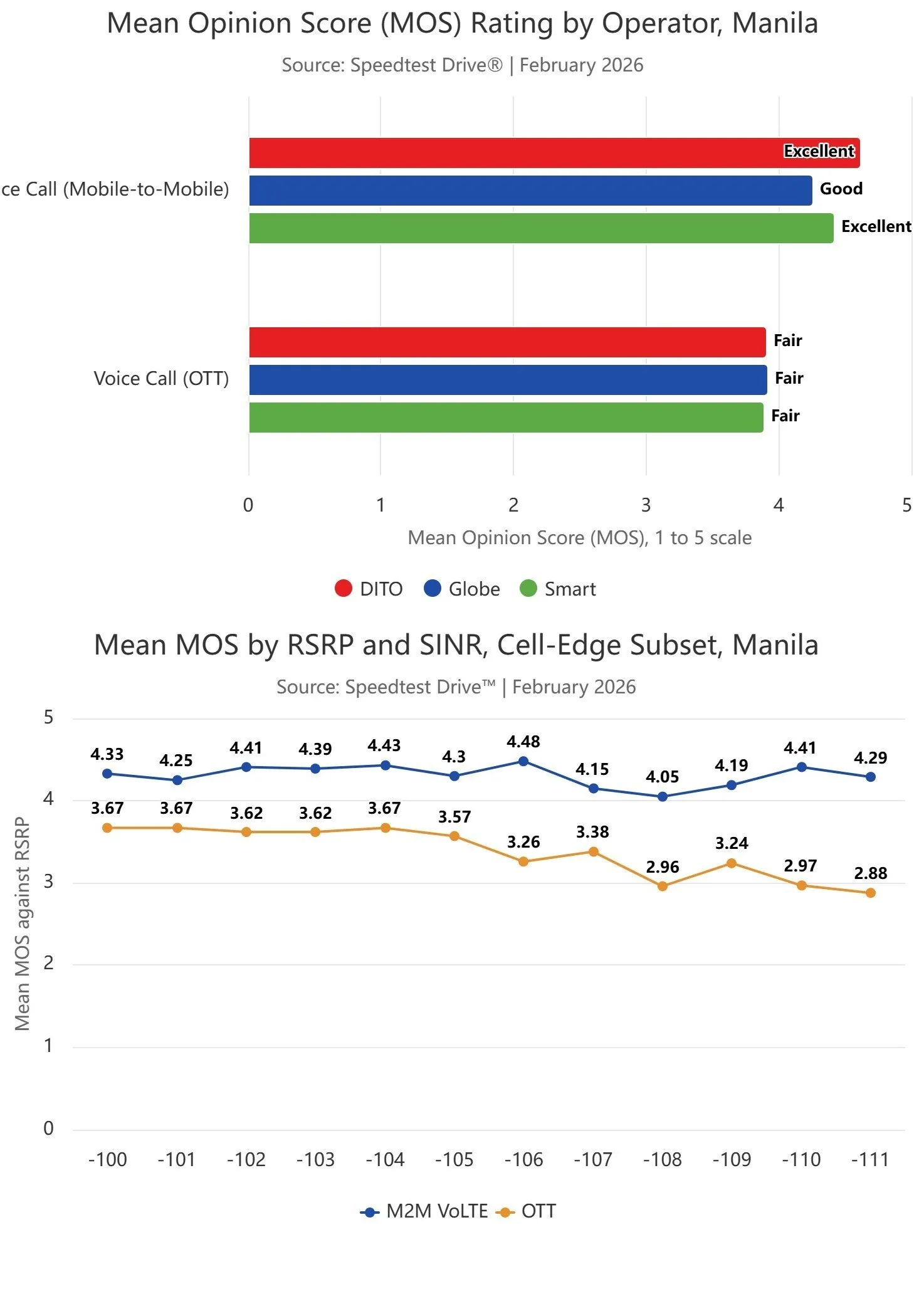
MANILA, Philippines , July 27, 2026 -- Ookla s comprehensive controlled network test reveals that traditional mobile operator networks deliver a measurably superior voice experience compared to Over-the-Top (OTT) applications like WhatsApp, particularly in critical areas such as audio fidelity, weak signal resilience, and call reliability. The study, which evaluated the networks of the Philippines three major mobile operators Smart Communications, Globe Telecom, and DITO Telecommunity , demonstrates that carrier-managed VoLTE infrastructure remains the gold standard for consistent, high-quality communication, outperforming OTT voice services.

Aolani and Rafay Collaborate on One of the Industry's First NVIDIA DSX OS Deployments on NVIDIA GB200 NVL72 Infrastructure
news
Jul 27, 2026 1 min

Aolani and Rafay Collaborate on One of the Industry's First NVIDIA DSX OS Deployments on NVIDIA GB200 NVL72 Infrastructure

The collaboration demonstrates how next-generation AI infrastructure can be transformed into production-ready AI platforms for enterprise and cloud providers. SUNNYVALE, Calif. and SINGAPORE , July 26, 2026 -- Rafay Systems , a leading platform provider for modern infrastructure and AI workloads and a member of NVIDIA Inception , today announced a strategic collaboration with Aolani to deliver one of the industry s first deployments of NVIDIA DSX OS running on NVIDIA GB200 NVL72 infrastructure, helping demonstrate how next-generation AI infrastructure can move from installation to production-ready AI services.

TECNO Unveiled as Title Sponsor of The SAFF Championship Bangladesh 2026, Bringing AI Innovation to South Asian Football
news
Jul 25, 2026 1 min

TECNO Unveiled as Title Sponsor of The SAFF Championship Bangladesh 2026, Bringing AI Innovation to South Asian Football

As Official Title Sponsor, TECNO joins hands with SAFF to inspire the next generation through football, innovation, and meaningful fan experiences. DHAKA, Bangladesh , July 25, 2026 -- TECNO, an AI-driven innovative technology brand, officially announced its title sponsorship of the SAFF Championship Bangladesh 2026, South Asia s premier international football tournament, during the tournament s official launch ceremony in Dhaka. Scheduled to take place from 4 17 November 2026, the championship will bring together South Asia s leading national teams, celebrating the region s passion for football while strengthening friendship, sporting excellence, and regional unity.

Tony Jaa Becomes GAC's 30-Millionth Customer - GAC Wins Global Trust with "True Craftsmanship"
news
Jul 25, 2026 1 min

Tony Jaa Becomes GAC's 30-Millionth Customer - GAC Wins Global Trust with "True Craftsmanship"

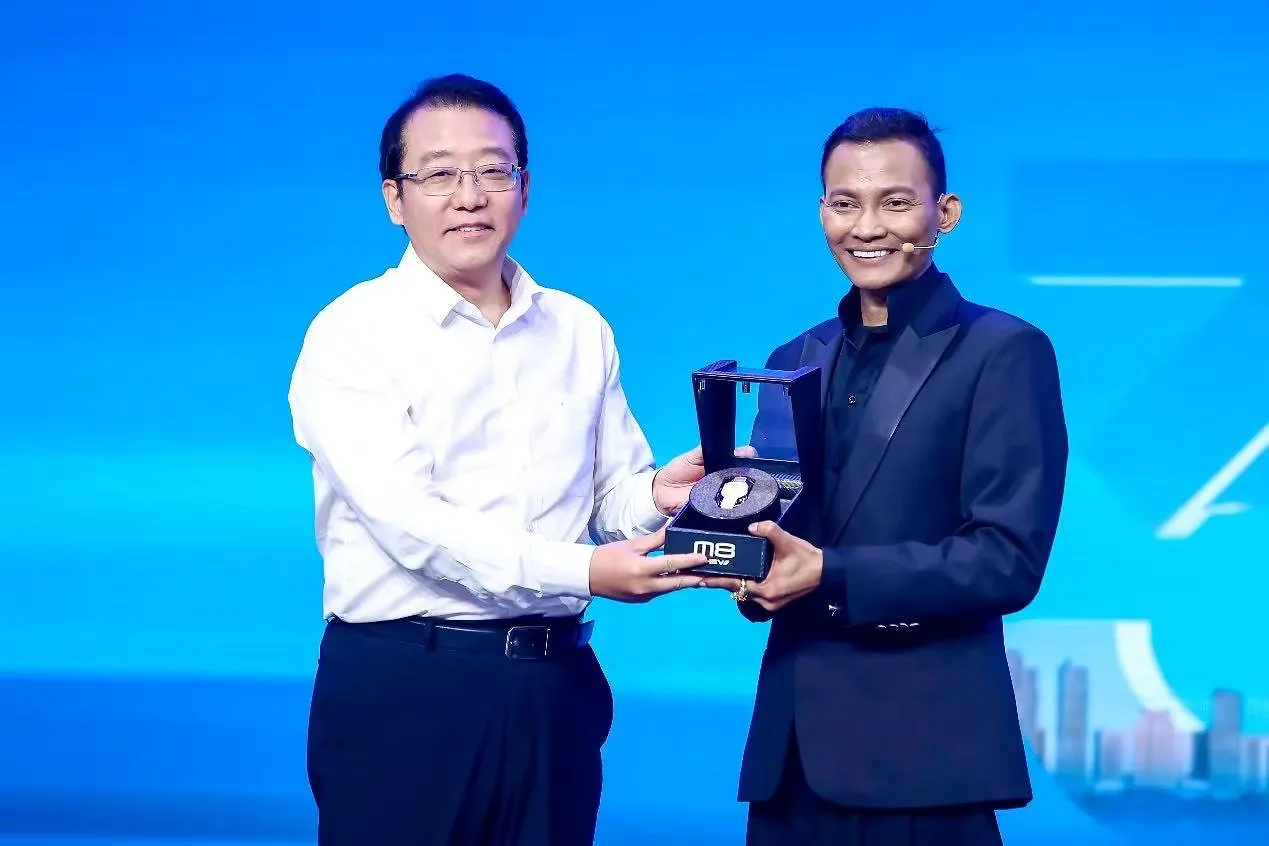
GUANGZHOU, China , July 25, 2026 -- On July 16, at the roll-off ceremony for GAC s 30-millionth vehicle, Feng Xingya, Chairman of GAC Group, handed over the key to the right-hand-drive GAC M8 PHEV (named GN8 overseas) to Tony Jaa. The milestone vehicle is headed straight for overseas markets. Thai action superstar Tony Jaa s choice reflects the trust of 30 million customers worldwide. That trust is built not on showmanship, but on GAC s solid manufacturing true craftsmanship.

From China Mobile's Call Upgrade to the Commercial Launch of "Calling + AI" by Leading Operators: AI Is Reshaping the Value of Native Calling
news
Jul 25, 2026 1 min

From China Mobile's Call Upgrade to the Commercial Launch of "Calling + AI" by Leading Operators: AI Is Reshaping the Value of Native Calling

BEIJING , July 25, 2026 -- On June 15, 2026, China Mobile announced a comprehensive upgrade to its traditional calling services, ushering in a next-generation calling experience defined by HD, intelligence, and security. This milestone not only marks a major leap in telecommunication innovation but also reflects a global, inevitable shift: the transformation of basic communication into intelligent, inclusive services. Breaking Experience Barriers and Redefining the Paradigm of Basic Calling